

Categorie

VIA IN PAD
VIA IN PAD
Via in Pad (VIP) Plated Over (VIPPO)
Increasing signal speeds, PCB functional density and PCB layer, thickness are increasing the challenges associated with PCB design, especially with respect to the signal integrity. These constrains have forced chip manufacturers to produce fine pitch chips (BGA, QFN, flip chips…), and PCB designers to use Via in Pad (VIP) Plated Over (VIPPO) structures in conjunction with traditional designs, such as dog bone traces, microvias, skip vias and pad-with-trace along with incorporating VIPPO in order to achieve routability and signal integrity requirements.
What’s Via in Pad?
When considering technology in PCB fabrication or PCB design, Via in Pad entails a PCB design to boost PCB density. This enables higher component density, especially in BGA and SMT areas. It can also be defined as the Pad having plated holes that link copper tracks layer to another. High-density PCB multi-layer can include blind vias, which can only be seen on one surface. It can also have buried vias, which can be seen on neither, a concept known as micro vias. The broad and advent utilization of small pitch devices and the need for finer size PCBs causes a new issue. The only solution to these issues is using the current PCB technology "via in pad'.

The use of via in pad technology helps minimize inductance and boost the density while using finer or smaller pitch package. The strategy employed here introduces directly via under the contact pad of the device. This approach gives room for higher density components and boosts the routing process. However, the technology offers the designers excellent PCB space savings. For instance, traditional devices fan-out introduces four components. With via in Pad, the board uses up to six components. If you are looking forward to getting intermediate density, you can consider filled via in Pad. It has an intermediate cost, unlike using buried or blind vias. Some of the key advantages associated with using the via in pad technology are:
1.Fan out fine pitch (less than 3mil) BGAs
2.Meets closely packed placement requirements
3.Better thermal management
4.Overcomes high speed design (HSD) issues and constraints i.e. low inductance
5.No via plugging is required at component locations
6.Provides a flat, coplanar surface for component attachment
However, there are some disadvantages associated with this technology. The most prominent and worrisome is the cost impact associated with adopting a new technology. PCB manufacturers and suppliers identified two primary cost drivers associated with specifying via in pad technology: Additional HDI PCB manufacturing process complexity and the underlying material cost for the conductive fill.
Specifically, via in pad technology adds 8 to 10 steps to the PCB manufacturing process while via filling cost is a function of the via size and actual number of via instances on any given design. However, the reduction in layer count realized by using via in pad technology compensates for the added cost associated with this process.
Via-in-Pad Fabrication Process
The Via in Pad technology proves to be a good technique to save real estate while making the layout of the PCB thus allowing denser PCBs. Here we list the main Via in Pad fabrication process for thru-hole PCB boards as below.
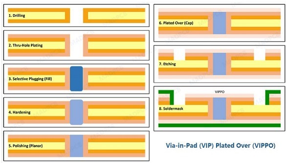
Maybe you find this is via in pad process is for thru-hole boards. Yes, but similar. In Microvia in Pad Process, the required selective microvias need to be fully filled plugged (/filled) with epoxy ink, then planarized, plated-over to get invisible capped microvia surface.
Manufacturable Via in Pad Technical Parameters
Solder Mask Filled or Epoxy Filled?
Solder mask cannot be used for filling the vias (microvias) in pad when forming Via in Pads since removing solder mask clearance from the SMT pad would make it un-solderable. In the solder mask filling, there was concern that nearby vias might wick away (straw and suck) some solder paste from a pad, so of course this is an even greater concern when the via is within the pad itself. In this case, MADPCB’s PCB production team will selectively fill the vias with an epoxy material but not solder mask before the surface finish is applied, which requires some additional cost and lead time compared to standard vias.
Conductive or Non-Conductive Epoxy Filled?
The epoxy is most often a non-conductive substance, since conductive substances expand much more quickly with heat, which can be troublesome during the reflow soldering process. Non-conductive filling does not impede the via’s ability to conduct electrical current, since the walls are still plated with copper just like any other via. In cases where the via must carry out a lot of current or heat through the PCB board, conductive epoxies are available as well. When the via in pad is plated through and then filled with a conductive or non-conductive epoxy plugging ink, the epoxy ink is then planarized to create a flat surface and plated over to get a fully filled and capped vias in pads.
When you send inquiry with PCB design files to GWT for quote, it would be helpful to note the presence of any vias within component pads. These will be taken into account for the pricing and lead time you see on your quote, and the CAM engineer can help you to determine if specific vias on your board will require filling of any kind.
Not Filled or Filled Via in Pads?
If vias in pads do not be filled, your assembled board will likely be missing connection between some of the BGA balls and the board. If you placing the via in the BGA pad, your only option is to have the vias filled and plated over at the PCB manufacturing house. If you placing the vias between the pads, you have two options. You can put soldermask dams on the short trace between the pad and the open via. This will prevent solder paste from migrating. The other, and the better, option is to cap the vias with solder mask. This gives a bit of extra protection in case of any of the solder mask dams are too thin or chip off. Just make sure you cap these things on the solder side. If you cap them on the back, solder paste can still spread on the trace and partway into the via. That still puts the electrical and mechanical connection at risk.
0users like this.
