

Categorie

MICROVIA
MICROVIA
The miniaturization trend – more complex technology that needs to fit in a smaller surface – affects not only the electronic product but the circuit board itself. Such demands drive the need for more advanced printed circuit boards and the use of microvias.
What is a microvia hole?
According to the new definition within IPC-T-50M a microvia is a blind structure with a maximum aspect ratio of 1:1, terminating on a target land with a total depth of no more than 0.25mm measured from the structure’s capture land foil to the target land.

The IPC-6012 also defines the structure of a Microvia.
1.The Microvia is a blind structure with a maximum aspect ratio of 1:1 between hole diameter and depth, with a total depth of no more than 0.25 mm, when measured from the surface to the target pad or plane.
2.Typically GWT considers the dielectric thickness between surface and reference pad to be 60 – 80um.
3.The diameter dimensions of the microvia have a range of 80-100 microns. The typical RATIO is between 0.6: 1 to 1: 1, ideal 0.8: 1
Design guidelines for microvias
Below are extracts from our HDI design guidelines showing some details for type I, II and III constructions. However, one important point to note regarding type III construction is that stacked structures should be limited to 2 layers of microvia and, where possible, avoid stacking on buried holes.
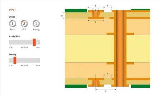
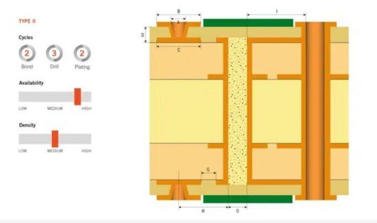
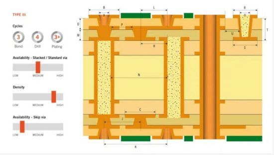
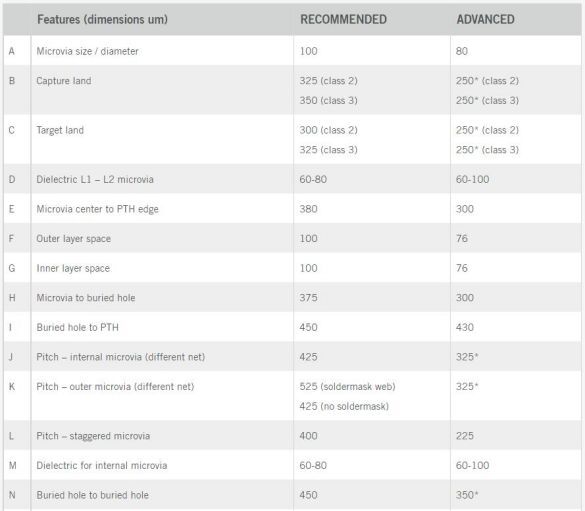
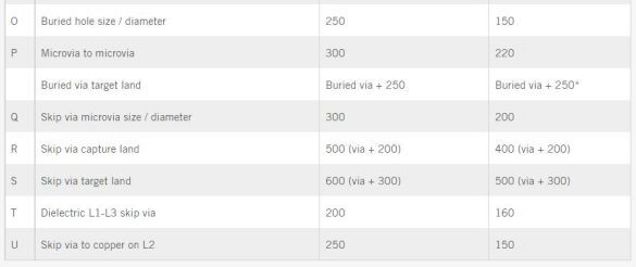
* For design tighter than the given value, please contact to discuss specific projects case by case.
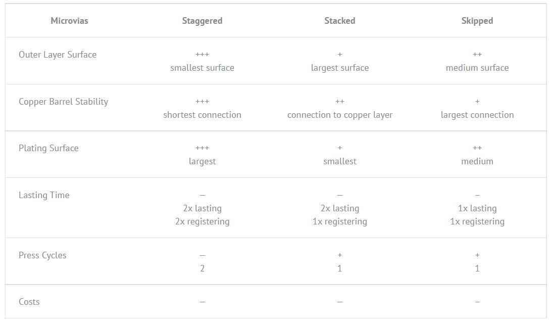
Stacked or staggered microvia constructions?
Although we continue to see both stacked and staggered designs (see image below), there has been an IPC test committee established to look into the reliability of stacked microvias for high performance products.
Failures, post manufacturing, have been reported over recent year and the problems appears to manifest itself at the bottom of one microvia and the metallurgical junction of another via or copper layer. What is known is that this trend is seen in complex stacked microvias, but not in staggered vias.

The data compiled so far seems to suggest that stacked microvias of 3 or more layer of microvia are much more likely to experience failure than staggered via structures. It is worth pointing out that the numbers are low in terms of % failure, yet when compared to similar failure rates in staggered via holes there is a marked difference.
The rule of thumb, or recommendations at this point in time seem to be that the stacked structures should be limited to 2 layers of microvia and where possible avoid stacking these on a buried via hole. If the design calls for a third layer of microvia, then this third layer shall be tracked away from the 2 microvia stack and completed as a staggered design.
Comparisons of Staggered, Stacked and Skipped Microvias
Microvia Reliability
The reliability of HDI structure is one of the major constraints for its successful widespread implementation in the PCB industry. Good thermo-mechanical reliability of microvias is an essential part of HDI reliability. Many researchers and professional have studied the reliability of micro vias in HDI boards. The reliability of microvia depends on may factors such as microvia geometry parameters, dielectric material properties, and processing parameters.Microvia reliability research has focused on experimental assessment of the reliability of single-level unfilled miicrovias, as well as finite element analysis on stress/strain distributions in single-level microvias and microvia fatigue life estimation. Micro-via failures identified from the research include interfacial separation (separation between the base of the microvia and the taget pad), barrel cracks, corner/knee cracks, and target pad cracks (also preferred to as micro-via pull out). These failures result from the thermomechanical stresses caused by coefficient of thermal expansion (CTE) mismatch, in the PCB thickness direction, between the metallization in a microvia structure and the dielectric materials surrounding the metal.
0users like this.
