

PCB design guidelines
-
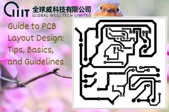
Guide to PCB Layout Design: Tips, Basics, and Guidelines
Guide to PCB Layout Design: Tips, Basics, and GuidelinesAn efficient and well-structured PCB layout is crucial for ensuring optimal performance, signal integrity, and reliability of electronic devices...
-

What are microcontrollr and microprocessor?
What are microcontrollr and microprocessor?In the landscape of computing hardware, the terms “microcontroller” and “microprocessor” often generate confusion due to their overlapping functions. However...
-
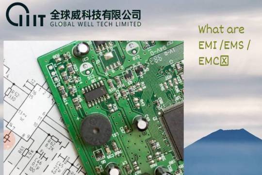
What are EMI /EMS /EMC?
What are EMI /EMS /EMC?Electromagnetic Interference (EMI), Electromagnetic Susceptibility (EMS), and Electromagnetic Compatibility (EMC) are crucial concepts in ensuring the smooth functioning of devi...
-
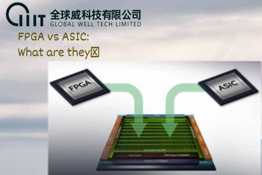
FPGA vs ASIC:What are they?
FPGA vs ASIC:What are they?What is FPGA?Field Programmable Gate Arrays (FPGAs) are reprogrammable semiconductor devices. They boast configurable logic blocks and interconnects, allowing users to custo...
-

IoT: what is the impact on PCB Design & Manufacturing?
IoT: what is the impact on PCB Design & Manufacturing?The term IoT, or Internet of Things, refers to an infrastructure comprising several electronic devices connected to the Internet. Smart devices, r...
-
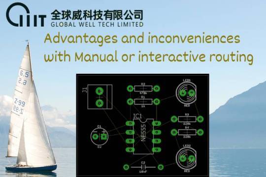
Advantages and inconveniences with Manual or interactive routing
Advantages and inconveniences with Manual or interactive routingLayout definition is certainly one of the most complex operations that the designer has to face when developing a PCB board (PCB). This ...
-
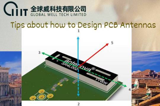
Tips about how to Design PCB Antennas
Tips about how to Design PCB AntennasPCB antennas come in various shapes and sizes and designing them is a crucial aspect as they have numerous applications. The techniques for designing a PCB antenna...
-

Introduction about PCB footprints
Introduction about PCB footprintsWhat is PCB footprints?The PCB footprint defines the physical interface between each electronic component and the PCB board, providing essential information for the as...
-
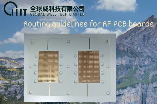
Routing guidelines for RF PCB boards
Routing guidelines for RF PCB boardsMain guidelinesA first aspect to take into consideration during RF signal routing concerns the impedance matching. A circuit without impedance matching, in fact, ge...
-

PCB design for Embedded Systems:the main fabrication techniques to create a printed circuit for embedded applications.
PCB design for Embedded Systems:the main fabrication techniques to create a printed circuit for embedded applications.1.PCB sizeSize is one of the most obvious and important constraints in PCB design....
-

What to do when PCB Design Under Space Constraints?
What to do when PCB Design Under Space Constraints?Some of the techniques of Space constraints can be resolved by making sure the components that are placed are having absolute clearance for other com...
-
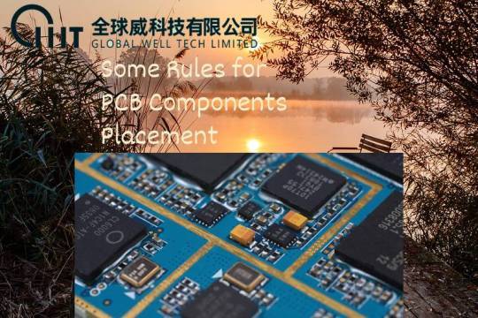
Some Rules for PCB Components Placement
Some Rules for PCB Components PlacementComponent placement is one of the very first stages of PCB design and must be approached with the utmost care in order to avoid costly rework and waste of time. ...
-
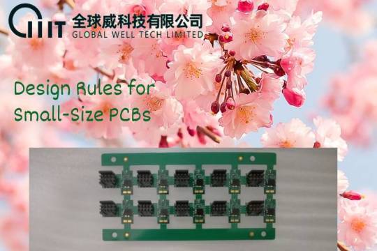
Design Rules for Small-Size PCBs
Design Rules for Small-Size PCBsReducing the size of an electronic circuit has multiple advantages, in addition to saving space.However, designing a small PCB can be a major challenge for many designe...
-
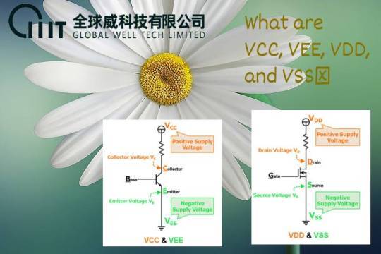
What are VCC, VEE, VDD, and VSS?
What are VCC, VEE, VDD, and VSS?The terms VCC, VEE, VDD, and VSS are used in relation to power supply voltages. Here are their meanings and differences.1.VDD• VDD is used as the positive supply voltag...
-
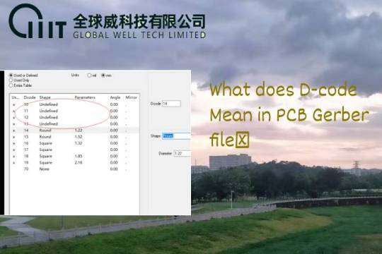
What does D-code Mean in PCB Gerber file?
What does D-code Mean in PCB Gerber file?1.Introduction for PCB Gerber filePCB Gerber file is a universally accepted data format in the PCB industry, serving as an intermediate medium for designing an...
-

Five PCB Design Hints
Five PCB Design HintsPCBs used in automotive industry not only require the selection of a suitable material, but also a careful design that guarantees both the fulfillment of the requirements imposed ...
-
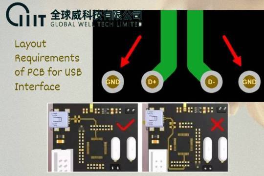
Layout Requirements of PCB for USB Interface
Layout Requirements of PCB for USB Interface1.The USB interface should be positioned close to the edge of the board or the structure positioning, and protrude out of the edge of the board to a certain...
-
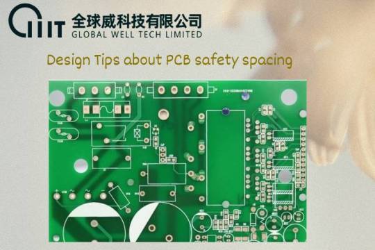
Design Tips about the PCB safety spacing
Design Tips about the PCB safety spacingThere are many places in the PCB design that need to consider safe spacing. Here, for the time being, they fall into two categories: one is electrical-related s...
-
The Significance of Board Size in PCB Design
The Significance of Board Size in PCB DesignGerber files are the de facto standard in the PCB manufacturing industry for conveying design information to fabricators.They serve as a universal language ...
-
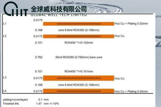
4-Layer PCB Stackup in PCB Design
4-Layer PCB Stackup in PCB Design4-layer PCB stackup refers to a PCB board configuration comprising four conductive materials separated by insulating layers. This stackup offers more flexibility and f...


