

Categorie

VIA Covering
VIA Covering
Several technical or production-related demands require the covering / sealing of vias. These types of Via covering are possible:
*Via Plugging (partially filled)
*Via Tenting (simple covering)
*Via Filling (completely filled)

Via Plugging (partially filled)
IPC 4761 Type III: Plugged Via
The via is partially filled with non-conductive paste.
One-sided: Type III-a
Double-sided: Type III-b
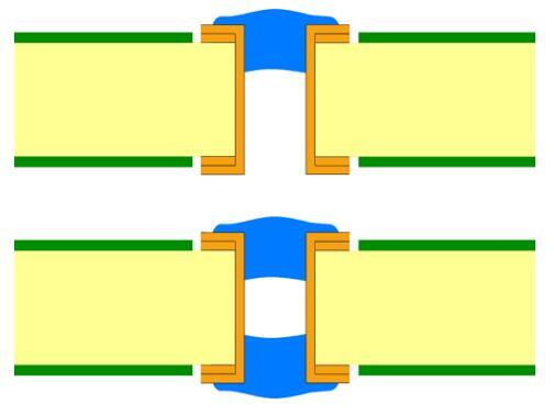
IPC 4761 Type IV: Plugged & Covered Via
The via is partially filled with non-conductive paste and overprinted with normal solder-stop, afterwards.
One-sided: Type IV-a
Double-sided: Type IV-b
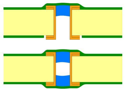
GWT recommends one-sided plugging (Type III-a / Type IV-a) as there is a chance of cracks through encapsulated gas while soldering double-sided plugged vias.
Application
1.Protection of solder floating up to the component side
2.Enables vacuum-adaption for production
Designation
Copy the vias to be filled into an additional layer and define that layer with your order.
Via Tenting
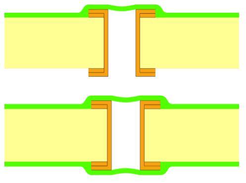
IPC 4761 Type I: Tented Via
The via is completely covered with dryfilm solder-stop.
One-sided: Type I-a
Double-sided:Type I-b
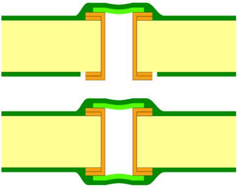
IPC 4761 Type II: Tented & Covered Via
The via is completely covered with dryfilm solder-stop and overprinted with normal solder-stop, afterwards.
One-sided: Type II-a
Double-sided:Type II-b
Application
1.Protection of solder floating up to the component side
2.Enables vacuum-adaption for production
3.Covering of critical vias, e.g. beneath BGA
IPC 4761 Type V: Filled Via
The via is filled completely with non-conductive paste.

IPC 4761 Type VI: Filled & Covered Via
The via is filled completely with non-conductive paste and overprinted with normal solder-stop, afterwards.
One-sided: Type VI-a
Double-sided: Type VI-b

IPC 4761 Type VII: Filled & Capped Via
The via is plated-through and cleaned - afterwards a non-conductive paste is forced in and hardened - the ends are planarized, metallized and plated-over. Hence, the surface is planar and solderable.

This technology is mostly used for Via-in-Pad solutions and is also applied for stacked und staggered (Micro-)vias. Via Plugging faciliates routing of additional conductor traces between BGA vias amongst other things.
Filled & Capped Vias are also possible for Blind Vias.


Application
1.Space saving
2.Protection of solder floating up to the component side
3.Faciliates stacked und staggered Microvias for sequential build up multilayers (SBU)
4.Facilates Via-in-Pad Technology, e.g. for BGAs
Additional Information
Drills & Throughplating
Blind & Buried Vias
Design Parameters
0users like this.
