

Categorie

PTH & NPTH
PTH & NPTH
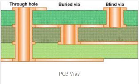
In PCB manufacturing, Through Holes are drilled from the top and go completely through the bottom of a PCB, these holes can be plated (PTH) or non-plated (NPTH). of a printed circuit board or flexible printed circuit, these can be plated (PTH) or non-plated (NPTH). With plated through hole, there is a conductive path from one side of the board to the other, or, no conductive path.
*PTH(Plated-Through Hole):The main characteristic of PTH is that, during the manufacturing process, after drilling, the boards a thin copper layer is plated onto the walls of the holes, providing them with electrical conductivity. In this way, after the PCB assembly manufacturing is finished, the link between the components’ leads and the copper traces has a lower resistance and better mechanical stability. Today, the most PCBs are double-sided, or multi-layered, and most of the through holes are plated. The components can connect to the required layers in the board. Plated-through holes can also be plated slots, plated half-holes (castellated holes), not always round in shape.
*NPTH(Non-Plated Through Hole ): From its name, this type of through holes no copper plated onto the walls of the holes, so the barrel of the hole has not electrical properties. They were very popular when printed circuits only has copper traces printed on one side, but their use decreased as the number of layers in PCBs increased. The main advantages of NPTH are that the manufacturing process for these simpler, and obviously quicker. Nowadays, they are frequently, but not exclusively, used as Tooling/Mounting holes: used to fix the PCB to its operational location. However, they can also be used for components mounting in some PCBs, like single-sided.
How to Lower Through Hole PCB Cost?
For standard PCBs, how to design the holes, annular rings and hole density will have effect on your PCB cost. Here are some ideas for reducing your cost.
1.Larger Holes: When it is feasible, use larger diameter holes and annular rings. To manufacture small holes, high precision machines are required; these machines always cost more to use so PCB fabricator often adds an upcharge for holes in diameter between 0.15mm and 0.3mm. To determine the added cost, you will need to contact the MADPCB to learn our policies about additional charges for hole sizes of standard printed circuit boards.
2.Larger Annular Rings: Minimum annular ring is a vital requirement that refers to through hole pads and vias only, and it is defined as the border of the hole’s and the pad’s minimum distance. That is, it is the copper rings smallest width the limits the hole. It is important to know that the cost of the PCB will be higher if the minimum annular ring is less than our standard requirements. A round through hole pad or via annular ring width is homogeneous around the hole, while the width of an oblong-shaped through hole is non-homogeneous. No matter round-, or oblong-shaped through holes, just keep in mind, using larger annular rings will decrease the PCB cost since high efficiency, and increase the PCB quality since no need to worry drilling tolerance or shaving rings.
3.Lower Hole Density Per Square Meter: No matter mechanical drilling or laser drilling, the machines have their own efficiency. High hole density per square meter, especially for PCB mass production runs, it will spend longer time to finish the drilling process, PCB fabrication house will charge additional drilling cost. If it is possible in your PCB design, decreasing the hole density per square meter will cost your less in cost.
0users like this.
