

PCB knowledge

PCB stack-ups
PCB stack-ups
Stack-up is an arrangement of insulating layers and copper. It is done prior to the layout design of the circuit board. In a multilayer printed circuit board (PCB), stack-up layers are silk screen, solder mask, high speed signal layer, signal layer, power plane, and ground layer. Designing a PCB stack-up is one of the most important factors for deciding the performance of the product. Therefore, it goes without saying that choosing the right and experienced manufacturer for designing a PCB stack-up is crucial.
Important Factors to Consider for PCB Stack-Up
Following are some important factors to be considered for a board stack-up:
1.The number of stack-up layers
2.The sequence of the layers
3.The spacing between the layers
4.The types and number of planes (ground and/or power) used
PCB Stack-Up Capabilities
We can provide you with different PCB stack-up designs based on your requirements. Following are the standard PCB stack-ups that we provide:
4 Layer
As the name suggests, a 4-layer PCB stack-up consists of 4-layer that are spaced at a uniform distance from each other. The internal layers are power and ground, whereas the external signal layers have orthogonal trace routing directions.
6 Layer
As far as EMC (Electromagnetic Compatibility) is concerned, a 6-layer PCB stack-up is preferred over a 4-layer one. Typically, a 6-layer PCB stack-up consists of two planes and four signal routing layers.
8 Layer
The EMC performance of an 8-layer PCB stack-up is better as compared to that of a 4- or 6-layer stack-up. An 8-layer PCB stack-up consists of four planes and four wiring layers.
The number of layers should be finalized only after taking into account the following factors:
1.The cost and number of signals to be routed
2.Whether the product meets Class A or Class B emission requirements
3.Whether the PCB is in a shielded or unshielded enclosure
4.EMC engineering expertise of the PCB designer
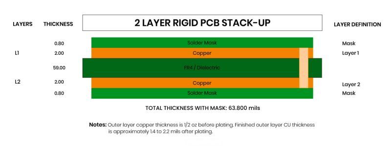
Some stack up for reference:


0users like this.
