

PCB assembly guidelines

GWT's Assembly capabilities -Sizing
GWT's Assembly capabilities -Sizing
In the PCB industry, there are many different sizing requirements that can affect the overall cost, quality, and turnaround time for a project. This section will discuss those sizing requirements that relate to the PCB assembly process specifically and GWT’s capabilities therein. For more information on sizing requirements for PCB Fabrication, see GWT’s DFM Guidelines.
1.Pad and Hole Sizes
It is generally most advisable to use the pad and hole sizes recommended by the datasheet for a given part, and GWT is generally capable of handling any such designs. It does sometimes happen that a datasheet does not give pad or hole information, and sometimes a PCB designer wonders about pushing beyond these recommendations to economize board space. In the latter scenario, this design decision should be explicitly stated in the assembly drawing for the project to avoid pre-assembly questions from GWT, and to ensure that GWT employs the correct quality controls during PCB assembly.
Where a design must deviate from datasheet suggestions, GWT’s minimum capabilities are as follows:
BGA Pad Sizing
GWT’s minimum capability for BGA Pad Size depends to some extent upon the surface finish used on the PCB (for more on surface finishes, see GWT’s DFM Guidelines).
--For LF-HASL, 12mil diameter is the absolute minimum
--For any other surface finish, 10 mil diameter is the preferred minimum & 7 mil is absolute minimum
GWT is able to control pad side tolerance for BGAs to within +/- 1.5 mil preferred, or +/- 1.2 mil minimum
SMT Pad-to-Lead Aspect Ratio
For surface-mount parts, the pads in a land pattern must be somewhat larger than the actual leads of the part to allow for solder to flow and form proper connections. When in doubt, designing the pads slightly larger necessary is always safer than designing them too small. The necessary pad-to-lead aspect ratio differs not only between package types, but also between the specific technology incorporated in given devices of the same package. As such, GWT would strongly recommend following datasheet recommendations for surface mount pad sizes. If no such information is listed in a given datasheet, then it is advisable to follow the sizing listed for a similar part

Figure 01-Minimum Ratio (C1 - Left) & Larger Ratio (C2 - Right)-Both acceptable
THT Hole-to-Lead Aspect Ratio
For through-hole parts, the diameter of the holes for assembly should be the diagonal of the cross-section for the lead to be installed

Figure 02-THT Hole-to-Lead Sizing – IPC-2222A
THT Annular Ring

2.Package Sizes
GWT can handle assembly of small passive packages down to 0201 resistors and capacitors to meet the
electronics industry’s growing demand for smaller products. Accurate automated assembly and meticulous
quality assurance checks allow these delicate components to be flawlessly installed, but it is still recommended to stick with larger sizes whenever possible for DFA purposes. The additional process which must be observed for the assembly of very small parts, coupled with the inherent production loss involved in handling them, means extra cost for the project that could be avoided by up-sizing passives to a more comfortable 0603 sizing.
On the other side of the package size equation, larger QFN, QFP, and BGA modules are sometimes required to perform very complex or demanding processes. GWT can handle the assembly of these parts as well, for parts up to 32mm, but some specific placement notes are strongly recommended for such components:
1. Large packages should not be placed in the center of a PCB,Since this is where the maximum bow & twist tends to occur,which can result in broken connections.

Figure 03- Bow & Twist on a Centrally-Placed BGA (Exaggerated for Clarity)
2. Large packages should be placed only on one side of the PCB. If they must be placed on both sides, they should not be in the same x-y positions (“on top of” each other), since this will greatly complicate X-Ray inspection and rework.
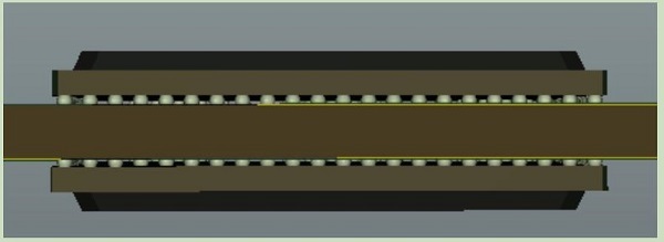
Figure 04-BGA Packages Placed "On Top Of" One Another
3.Pitch
GWT can handle assembly for fine pitch parts down to 0.4mm using regular processes; 0.35mm pitch is feasible but may require some additional cost for specialized quality control processes.
Certain BGA packages, known as “dual-pitch BGAs”, specify a different pitch for row-axis pads than for column axis pads; that is, vertical spacing between pads might be different than horizontal spacing between pads. GWT can handle dual-pitch BGAs as long as the above minimum pitch requirements are met.
0users like this.
