

Categorie

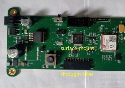
Through hole PCB Assembly
Through hole PCB Assembly
In through hole PCB assembly, the components are mounted on the PCB board by inserting their leads/terminals in holes that are already drilled through the PCB board. These terminals are then soldered manually or through reflow soldering to hold the component in place and connect it to the conductive path. One key thing to note about Through hole assembly is that it is not very efficient for multi-layer PCBs as it takes up board space on every layer. As a result, this type of assembly is usually found on single-layer PCBs.

The Through Hole Soldering technique was the primary method which was used to add components on a PCB till the emergence of Surface Mount Technology. Components soldered using the Surface Mount Soldering technique (SMT) do not have leads and can be directly mounted on the surface of the PCB. In addition to this, the components of SMT are smaller in size and can be mounted on both sides of the board.
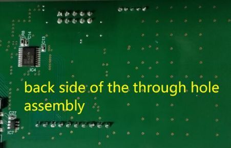
The Through Hole Soldering technique requires the drilling of holes onto the PCB through which the leads can be inserted and can be soldered to the other side of the board. As a result, this process can be more expensive and time-consuming when compared to using Surface Mount soldering techniques.
Through-hole Soldering techniques are still used for testing and prototyping. They can also be used in environments that have high mechanical and thermal stress, as the leads going through the board provides a stable structure. However, most applications today use surface mount soldering techniques.
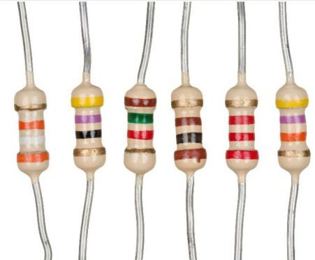
Some examples of Axial Components:
--Resistors
--Carbon film resistors
--Diodes
--Inductors
--Capacitors
Radial Components: Radial leads are placed parallel to each other from the surface of the component. When Radial Leads along with their components are placed on a board, they are positioned perpendicularly to the board occupying lesser space making them useful in high-density applications.
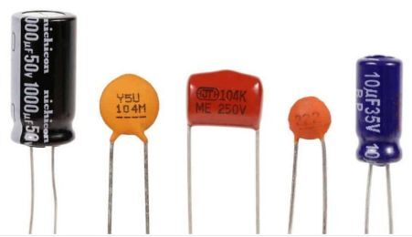
Some examples of Radial Components:
--MOSFETs
--LEDs
--RGBs
--Photoresistors
--Photodiodes
--Ceramic Capacitors
Steps to Perform Through Hole Soldering:
Step 1: Cleaning the PCB and Components:
The PCB and the electronic components are first cleaned with isopropyl alcohol and then wiped dry. The PCB must be free of dirt or dust.
Step 2: Bend the Leads

If an Axial Component is used for mounting onto the PCB they are bent initially using a plier so that they fit perfectly onto the PCB. If a radial component is being used it can be inserted directly into the holes of the PCB.
Step 3: Place the Component and Cut the Leads
After the electric component is bent, they are then inserted into the holes of the PCB according to the design schematics and excess lead is cut-off. It must be observed that the component lies flat on the PCB
Step 4: Soldering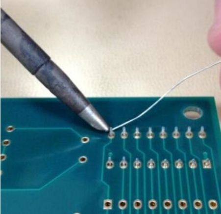
The Important rule for through-hole soldering is that the flux can be applied to both sides of the board, but the solder must be applied to only one side. Applying FLUX to both sides of the PCB will help keep the soldering area clean and help with heat conduction. One must ensure to apply solder only to the underside of the board.

0users like this.
