

Categorie

Lead-free PCB assembly
Lead-free PCB assembly
Lead-free PCB assembly means PCB assembly that uses no lead during any phase of manufacturing. Lead is traditionally used in the PCB soldering process. However, lead is toxic and is therefore hazardous to humankind. Considering its consequences, Restriction of Hazardous Substances (RoHS) directive by the European Union prohibits the use of lead in PCB assembly processes. The replacement of lead with less toxic substances causes little differences in the PCB assembly process.
Surface Finishes for Lead-Free PCB Assembly
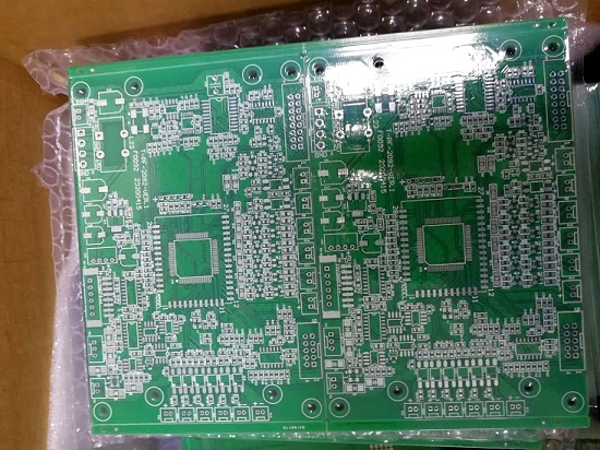
For lead-free PCB assembly, the surface finishes for PCBs can be ENIG, OSP, ENEPIG, lead-free HASL, gold plating, immersion silver, immersion tin, and carbon ink.
For flexible PCBs, lead-free HASL can't be used, and you can use OSP or ENIG to replace it.
*OSP is easy to oxidize, and if the circuit boards are not assembled immediately after PCB fabrication, the PCB manufacturer has to package the circuit boards panel by panel in vacuum bags. Only when placing the lead-free PCBs on the SMT lines, should they be unpacked. And OSP PCBs can't be baked before PCB assembly. Also, take note that the storage period for OSP PCBs is within 30 days. If the storage period is beyond 30 days, return the boards to the PCB manufacturer to apply OSP again.
*ENIG and ENEPIG have excellent solderability and are used for high-reliability PCBAs. Gold plating is usually used for gold fingers/edge connectors on the PCB edges used for the connection.
*All surface finishes are available from the advanced PCB manufacturer GWT. And we can make selective OSP, lead-free HASL, and ENIG on the lead-free PCBs.
Solder Paste for Lead-Free PCB Assembly
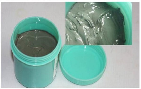
The lead-free solder paste is composed of Sn/Ag/Cu/Bi alloy powder and paste. Lead-free solder paste follows the RoHS directive and is in green bottles. Solder paste is stored at 2°C to 8°C and used at 22°C to 28°C.
How is solder pasted used in the lead-free PCB assembly process?
For OSP PCBs, the solder in the solder paste melts and forms metallic compounds with copper pads. For PCBs with other surface finishes, the solder, surface finish, and copper pads form metallic compounds. And the flux in the solder paste activates the solder and evaporates away.
Reflow Soldering Temperatures for Lead-Free PCB Assembly
Reflow soldering is the most important step of lead-free PCB assembly. The reflow temperatures follow the lead-free reflow profile and include the preheat stage, soak stage, reflow stage, and cooling stage. For lead-free FR4 PCBs, the peak temperature range is 240℃ to 270℃. Compared with lead-containing PCB assembly, the reflow soldering temperatures are about 30℃ higher.
--Profiling:
Profiling is a prototype resembling process. The manufacturers take a finished lead-free PCB as a prototype. This can be a functioning actual PCB or a non-functioning PCB or dummy parts. The stencils for assembly are traced by profiling. The lead-free assembly designs are compared to prototypes in order to ensure its compatibility for the assembly.
--Solder Paste-Inspection:
Since the lead-free solder joint gives a metallic appearance, which is very different than a lead-based solder, it is important to inspect meticulously. The PCB profile and solder paste are inspected under IPC-610D standards to ensure the lead-free solder joints will be firm and solid. The moisture level is also tested in this step because, in lead-free soldering, the board is exposed to a high level of moisture as compared to traditional soldering.
--Bill of Material (BOM) and Component Analysis:
In this process, the customer has to verify the Bill of Material (BOM) in order to make sure the components are made of lead-free material. Lead-free components are prone to moisture therefore should be baked in the oven by the manufacturer. Once the prerequisite steps are performed, the actual lead-free assembly begins.
Active Assembly Steps
In the active assembly process, the PCB assembly actually takes place. The steps involved in the active lead-free assembly are detailed as follows.
--Stencil Placement and Solder Paste Application:
In this step, the lead-free stencil from the profiling stage is placed on the board. Then the lead-free solder paste is applied. Generally lead-free solder paste material is SAC305.
--Component Mounting:
Once the solder paste is applied, the components are mounted on the board. The component placement can be done manually or by using automated machinery. This is a pick and place operation but the components used are required to be confirmed and labeled in the BOM verification stage. The machine or operator picks the labeled component and places it to the designated location.
0users like this.
