

PCB design guidelines

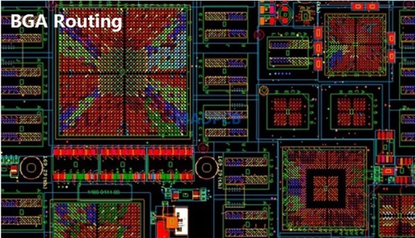
BGA Routing Guidelines
BGA Routing Guidelines
As market demand for smaller electronic devices with greater functionality continues to increase, PCB designers at GWT are turning more and more to ball grid arrays (BGAs). Using BGAs allows PCB boards with greater functionality to be used in progressively smaller products. BGAs are intended for multilayer PCBs where vias are used to route signals between different copper layers. BGA routing in complex PCB layout design seems not easy.
Vias add flexibility to the PCB design process and complexity to the PCB fabrication and assembly process. Just as there are tolerance considerations, placement restrictions and best design practices for components and traces, so too for multilayer routing BGA connections and using vias. By applying BGA routing best practice, you can ensure that your PCB boards are less susceptible to common challenges that can impact manufacturability and functionality.
BGA Routing Challenges
BGA routing presents unique challenges that must be considered as you design your printed circuit board. The most significant of these involve ensuring the signal integrity, manufacturability and reliability of your board.
1.Signal Integrity: A key signal integrity issues is impedance control, which affects transmission and reflections. The impedance can be controlled by matching trace widths between forward and return lines, using the appropriate dielectric thickness and installing a reference plane between signal layers. Installing reference or ground planes between adjacent signal traces is also effective in minimizing crosstalk. When the signals are on the same layer, maintaining the spacing between traces is key. Check SI Analysis.
2.Manufacturability: In addition to determining the number of layers (signal and reference) to optimize signal integrity, you need to consider the manufacturability of the BGA scheme. There are specific restrictions and guidelines depending on how the BGA connections are routed with each other and externally. The number of layers, pitch angles, via sizes, type of hole drilling and other concerns are limited by the capabilities of the PCB board manufacturer.
3.Reliability: The reliability of your PCB board depends on board construction quality and synchronization of your design with the capabilities of your PCB manufacturer by employing good DFM (design for manufacturability) practices. Not synchronize or push the limits too far can result in PCB boards that don’t function as designed or may fail at some point once deployed in the field. Copper weight, solder mask thickness, coverlay thickness, and copper grain structure are material issues that cause failure in the field. Trace routing, including via choices, may also affect operation, leading to significant costs for recalls and replacement. Applying DFM check at MADPCB that incorporates these considerations on boards that include BGAs will align your PCB design with your board manufacturer’s capabilities. Let’s take a look at the options available along with BGA routing guidelines for vias that, if employed, will enhance the signal integrity and PCB manufacturability of your board.
4.BGA Via Options: The first step when designing your BGA routing scheme is to determine the number of signal layers required based upon your signal integrity considerations. A good rule of thumb is to use the equation: Number of Layers = Signals / (Routing Channels x Routing Per Channel). Remember to include reference planes when needed. With the quick-turn PCB design process, you can have your PCB layers up to 30 layers thick in a matter of days. The next step is to determine how to route your BGA signals. A number of options are available to you, but before settling on a strategy, you should consider how each may impact your PCB design
5.Through Hole Via: The most conventional method of connection through vias is through hole routing, which extends through the entire PCB board. Through-hole vias provide good signal integrity and are easy to implement but they require the most space.
6.Blind Vias: For routing directly from the BGA, blind vias are the alternative to through-hole. They offer the advantage of being able to incorporate stacked vias, staggered vias or a combination of these. Stacked vias allow for a denser design; however, staggered vias do not require the precise alignment that stacked vias do. From a PCB fabrication standpoint, the relaxed tolerances make it simpler to implement staggered vias. Finally, you need to determine whether to use via-in-pad routing or dog bone routing. There are tradeoffs in complexity and space that must be considered
7.Via-in-Pad Routing: The space requirements of through-hole vias can be minimized by using via-in-pad routing. For through-hole vias, the footprint is small and routing is easy, but the PCB design is complex. Blind vias, which improve signal integrity, present the tradeoff of being difficult to route. The steps necessary to implement standard via-in-pad add significant time to the PCB manufacturing and assembly process. This can double or even triple the manufacturing turnaround time. When using via-in-pad routing, minimum via hole and pad sizes are used to save space. Due to the precision needed, this may cause breakout. Breakout is when the via extends outside of the pad. This may be a significant issue if the breakout occurs in the direction of an incoming trace to the pad. In those cases, signal integrity loss may occur. An alternative to avoid this is dog bone routing.
8.Dog bone Routing: In this style of BGA routing, the via is offset from the pad and connected by a short trace, thus making a “dog bone” like shape. Dog bone routing does not need to be filled and capped process steps needed for via-in-pad routing, so it is less complex and faster to manufacture as opposed to via-in-pad. If the BGA pitch spacing allows it then this style of routing may be a better option than via-in-pad. However, designs can be complex and it can sometimes be unclear which style of via is appropriate. This is where the PCB design team of GWT can help. Your choice for BGA rouging may significantly affect the signal integrity and manufacturability of your PCB design. Additionally, your selection may add days to your board manufacturing turnaround time. By implementing BGA routing guidelines and best practices, you can ensure the manufacturability of your PCB board and reduce manufacturing time for your printed circuit boards.
BGA Routing Depends on Board Stackup and Layer Count
The first step in BGA routing has nothing to do with routing, it’s all about determining the number of layers you’ll need for routing. For high-ball-count BGAs, the number of layers can get very high and the layer thickness can become very small in order to support the required number of traces with controlled impedance. Fortunately, there is a simple process you can use to estimate the number of signal layers required to fully breakout traces from your BGA.
1.Count up the number of signal rows across the footprint of the largest BGA.
2.Divide this number by 2 to get the total number of rows that will require breakout routing.
3.Divide the number of breakout rows by 2 to get the number of signal layers required to support your signal rows.
This formula is used because each layer can support 2 rows of traces, as shown in the image below. In this image, we have a 27-row BGA (found by counting the number of vias vertically). However, most of the internal rows (about 19) are for different power buses and ground connections. This leaves a total of 8 signal rows that will require routing; dividing this by 4 gives us 2 signal layers that are needed for breakout routing.

Figure 01-The outer two rows on this Ethernet controller BGA are used for routing to RJ45 jacks and a DDR module.
The above layout shows an Ethernet controller (U1) being routed to multiple RJ45 jacks and a DDR memory module (U5). The top layer is shown above and is used to route differential pairs from the outer rows to the RJ45 jacks, as well as single-ended length-matched traces in a parallel bus to the DDR module (see the serpentine traces in the right side of the image). All of these traces are impedance controlled with a set width in Altium’s design rules. The remaining pads in the internal rows of the BGA are for power and ground; you can spot these as thick traces are used and to connect to vias, which then connect to polygons on the inner layers. Although this BGA has ~700 connections, only a small number are being used for routing signals, and the board shown above only required 6 layers to support all signals, power, and ground (2 signal, 3 power, 1 ground).
Read more about designing an HDI stackup for BGA routing.
If you’re using a rectangular BGA, use the short edge to count up your number of rows in the above formula. This is not typical outside of DDR and non-DDR SDRAM modules (see U5 above). In SDRAM modules, it’s typical to put a space between the rows of balls in the BGA to allow additional routing along the surface layer. One reason for this is that SODIMM RAM cards generally have limited layer counts (typically 4), so that leaves only 2 layers to route microstrips into dense SDRAM chips.
Once you’ve determine the layer count requirements, you can select a fanout style and size your vias.
Choose a Fanout Style
The standard BGA fanout style in a reasonably dense BGA (e.g., less than 1 mm pitch between balls) is a dog bone fanout, where small traces on the internal balls connect to vias between ball rows. This is the style used in the above image. When a denser BGA is used, the via and pad size may become so small that the fanout style will force the via to be placed directly in the solder pad for the BGA. In this case, the vias must be filled and plated over (called VIPPO) to create a solid copper pad for soldering during assembly. To determine whether via-in-pad or dog bone fanout can be used, you’ll need to determine the via size needed to route signals from the BGA footprint into the inner layer.

Figure 02-Dog bone fanout example for a BGA. Notice how each internal row is routed through a deeper internal layer.
Sizing Vias in BGA Routing
One important parameter that is sometimes overlooked in BGA routing and fanout is the size of the vias required to reach inner layers. There is an important aspect of reliability to consider here as defined in the IPC-6012 standards. As the pitch between balls gets smaller, the space available for the annular ring on internal vias also gets smaller. This eventually forces the via diameter to get smaller to continue complying with IPC-6012. Eventually, the via aspect ratio gets too large for the given via diameter, creating a DFM issue and forcing the designer to opt for blind/buried/staggered vias for routing internal rows.
At this point, the only way to relieve the DFM issue and ensure a sufficiently large annular ring is to just use via in pad. The cutoff for using via-in-pad vs. dog bone fanout is not so clear and depends on the ratio of the BGA solder pad size to the pitch, as well as the layer count and layer thickness. This is a complex problem that takes some experience as well as advice from an experienced fabricator.
Very High Density with VIPPO
In very dense BGAs with very high signal net counts, eventually the layer thickness will get so small that you might be able to route groups of differential pairs between balls. These boards may have 12 or more signal layers in order to support such a high number of signals required in the BGA breakout, but the trace width could be small enough so that you can still limit the number of layers to a manageable number. If you follow the above process and create a proposed stackup, you’ll be able to determine the required trace width and spacing needed to meet impedance and crosstalk requirements. Make sure to send your stackup in for approval with your fabricator before you start BGA routing, otherwise you’re risking a redesign once the PCB layout is finished.
One option is to take advantage of the input impedance of long transmission lines and use short sections to double BGA routing away from the external rows of the BGA footprint. This is shown below; the differential pairs in this image are routed so that the initial trace sections are very thin, allowing two traces to be routed between balls instead of one trace. This is only appropriate as long as the electrical length of the thin sections is sufficiently short, i.e., as long as the input impedance of the overall transmission line is not dominated by the impedance of the thin trace sections.
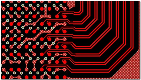
Figure 03-Dog bone fanout and BGA escape routing with thin trace sections.
0users like this.
