

PCB assembly guidelines

Wave Soldering
Wave Soldering
1.When to wave soldering
Wave soldering has fallen out of favour in the PCB assembly industry in recent years, at least in comparison to its past prevalence. The growing popularity of surface mount parts and high-density PCB layouts make reflow soldering the method of choice for a majority of projects, but wave soldering certainly still has its place. For legacy boards incorporating many through-hole components, as well as boards incorporating large connectors with very high pin counts, wave soldering is often still the most efficient method for PCB assembly.
GWT would recommend that clients design for reflow soldering as often as possible since wave soldering does require more strict controls in design than reflow soldering. GWT’s process engineering team performs a thorough analysis of the PCB design before any wave soldering job and will bring up any potential complications with a client in advance, but this does require additional time and cost compared to a reflow soldering project.
The following subsections briefly discuss some of the concerns that must be taken into account when designing a PCB that will be wave soldered.
2.Heat Profiles
Heat profile is one instance where wave soldering is actually less restrictive than reflow soldering. Though a similar level of high temperature is involved in both processes, the period of exposure to this high temperature is much shorter for wave soldering projects. A solder wave is passed rather quickly over a PCB, and temperatures exceed 100 °C for less than 10 seconds on average, whereas reflow soldering requires such high temperatures for close to 4 minutes.
3.Orientation & Shadowing
Component placement and orientation become crucially important for boards that are to be wave soldered due to an effect known as shadowing, which occurs when the body of one component blocks part of the solder wave and prevents it from contacting the pad of another component. In the case of a single-side through hole PCB, this issue is mostly avoided since there will be no component bodies on the solder side of the board. When designing double-sided or surface mount boards for wave soldering, orientation becomes a critical concern.
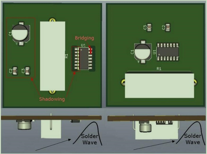
Figure 01-Poor Wave Soldering Orientation (Left) & Good Wave Soldering Orientation (Right)
Wave soldering is generally not recommended for QFP packages due to shadowing concerns, but if absolutely required, the package should be rotated 45° relative to the direction of travel for the solder wave. If the QFP package has an exposed central pad, wave soldering can not be used; similarly, wave soldering is not suitable for QFN, BGA, or other lead-less package types.
4.Pad Shapes
Pad shape is a concern for finer-pitch surface mounted parts when wave soldering is to be performed on a particular board. When the solder wave reaches the end of a part, the sudden change can cause excess solder to gather on the last few pads, potentially resulting in solder bridges. To protect against this issue, thieving pads are often added to the ends of these components to aggregate any excess solder as the wave passes.These pads should extend from the last functional pads that the solder wave will touch; it is common to use thieving pads for any surface mount packages other than passives on wave-soldered boards.

Figure 02-Thieving Pads on a SOIC-14 Package
Video-Wave soldering in GWT
0users like this.
