

PCB assembly guidelines

Testing Methods-Design for testing
Testing Methods-Design for testing
Design for Testing (DFT) is a specific subsection within Design for Assembly (DFA), focused on developing a product that can easily be measured and verified in terms of functionality. The following subsections provide an overview of the testing methods that GWT regularly employs after the PCB assembly process is completed. A working knowledge of these methods should help GWT’s clients decide exactly how extensive the testing process must be for each individual project, allowing for proper budgeting in terms of both lead time and overall project cost.
In addition to the testing methods outlined below, GWT performs 100% electrical testing on every bare board prior to assembly, so there is never any doubt in terms of whether a given issue stems from a PCB itself or the parts installed upon it. For more complete information on electrical testing processes, please see GWT’s DFM Guidelines document.
1.Automated Optical Inspection (AOI)
Automated Optical Inspection (AOI) is an efficient and accurate method for detecting PCB assembly errors before boards leave GWT’s production facility. This method employs high-resolution cameras and advanced image processing software to identify assembly errors such as missing or misplaced components, solder bridges, solder balls, or tombstones, to name a few;Click at here for more information on common issues.
Compared with visual inspection, AOI vastly improves error detection for complex circuit boards and volume production runs. The ongoing push for miniaturization in the electronics industry has effected a widespread adoption of AOI testing to maintain efficiency and accuracy in the post-assembly inspection process.
GWT’s quality assurance team provides visual inspection on all PCBs before they are packaged for shipping to the client. AOI is used in addition to visual inspection for orders meeting certain thresholds in terms of quantity or complexity. There is no extra cost or lead time involved with AOI inspection, as it is provided as a standard service for orders meeting the thresholds listed in the table below, and therefore included in the consideration for each PCB assembly quotation.
| Order Qty (Q) | Component Qty per board | Visual Inspection | AOI |
| Q<=10 | N/A | Yes | No |
| 10 | P<50 | Yes | No |
| 10 | P>=50 | Yes | Yes |
| Q>=50 | N/A | Yes | Yes |
Table 1 - AOI Thresholds
2.X-Ray Inspection
For designs including BGA, QFN, and other lead-less package types, connections to the PCB are formed beneath the body of the components themselves. As such, visual and AOI testing are not sufficient to verify a robust assembly, and GWT must employ X-Ray inspection in order to meet quality assurance guidelines. This service is included by default on any GWT quotations including the assembly of lead-less packages, such as those mentioned above.
Not only does X-Ray inspection detect issues in PCB assembly, but the analysis of an X-Ray image can help to determine the root cause of a given defect, such as insufficient solder paste, skewed part placement, or X-Rays penetrate the silicon of an IC package and reflect from the metal of the connections underneath, forming an image of the solder joints themselves that can be analyzed by advanced image processing software similar to AOI. Higher-density features in the captured area create a darker resulting image, allowing for quantitative analysis to determine quality of the solder joints and compare against industry standards.improper reflow profile.
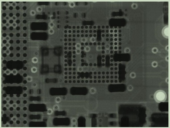
Figure 01-X-Ray Image of an Assembled BGA Package
3.Functional Circuit Testing-(FCT)
Functional circuit testing (FCT) is the final step in board-level production service, performed after AOI and visual inspections are completed. This procedure goes a step beyond other testing methods to verify not only the fabrication and assembly quality of a PCB, but the overall functionality of the project. In many cases, the electrical and optical inspections discussed in previous sections are sufficient, and FCT is not necessary, but it is a common procedure for projects which include IC Programming, and a requirement for those which include Conformal Coating. GWT’s comprehensive FCT procedure allows clients to be fully confident that they will receive a perfect product at the end of the production cycle.
The FCT process typically incorporates the use of a computer running specialized testing software. The computer is connected to specific test points on the assembled PCB and used in conjunction with test instruments such as digital multimeters, separate test PCBs, and communication ports. GWT’s test engineers prepare an individual test report form for each project subjected to FCT, which is filled out during the test procedure and kept on record, available to clients at their request.
Clients requiring FCT must submit a general test procedure and specific pass/fail requirements to GWT during the project’s quote stage, at which point the added labour cost and lead time is evaluated and included in the quotation. For higher-volume projects or those requiring very extensive testing, FCT will often require additional tooling cost to design and build a test jig, and this cost must also be included in the quotation. Due to the vast differences from project-to-project, these costs and timeframes must be determined on a case-by case basis.
GWT’s FCT stations are equipped with an adjustable DC power supply, a 200 MHz digital oscilloscope, a signal generator, an LRC multimeter, and a universal programmer, allowing for FCT on most embedded systems. After FCT, a GWT process engineer will issue a custom DFA form to the client, which offers design suggestions to improve functionality in future production runs. GWT’s quality assurance engineer will develop an 8D report for internal use, which focuses on assembly process improvements for GWT’s side of the equation.
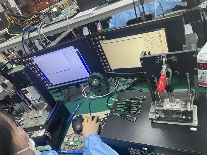
Figure 02 - GWT Test Engineer Performing FCT on an Assembled Board
0users like this.
