

PCB assembly guidelines

A Guide On PCB DFA (Design for assembly)
A Guide On PCB DFA (Design for assembly)
A Quick Introduction on Design for Assembly (DFA)
PCB assembly is the process of combining the PCB boards with other electronic components, such as connectors, enclosures, heat sinks, and much more for embedding into the end product. Knowing its immense significance, it is important to consider PCB assembly at the early designing process to get optimum results. If not, then you may end up with inadequate problems, such as limited board functionality, component conflicts, and more.
There are mainly two stages in PCB design for the assembly process. One is prototype pcb assembly and the other is production assembly. It is important to consider these two stages as part of DFA during the PCB board designing process.
1.Prototype Assembly: In this, the board prototype is assembled to check whether all the components are attached properly or not. The design should adhere to clearance as well as tolerance requirements. In addition to this, some other DFA measures should be observed during the design process. This may include adequate component spacing, precise component markings, appropriate application of solder mask, and more.
2.Production Assembly: Next, this assembly follows all the measures of prototype assembly and accounts for component reliability, volume production, component testability, and so on. The following DFA measures should be complied with in the prototype assembly.
--Appropriately defining quality controls
--Availability of components
--The board allowing penalization
--The layout withstanding extreme conditions
Essential PCB Design for Assembly Guidelines Analyzed
The designing of the PCB board plays an important role in every stage of the production process. Thus, various guidelines or important points can be drawn up. The following list covers the most important PCB DFA(design for assembly) guidelines.
1.Make use of standard and common components for your design assembly. This is because they are easily available for manufacturing. Using such components will help increase the quality, lower inventories, reduce overall costs, and so on. Avoid design components whose shelf life is about to end. Customized or unique parts lead to increased costs and delay your process.
2.Try to put all SMT components on a single side of the PCB board because putting SMT parts on both sides will increase costs for stencils and assembly challenges. Also, take the sizing of the components into account while placing the components. Uneven-sized parts will cause a problem for solderability.
3.Do not place components too close or too far from each other. Make sure no component should overlap as this may result in design changes in the PCB board. To prevent component spacing rules, ensure the PCB board design allows adequate space between the boundaries of components.
4.Heat dissipation is important to ensure the optimal performance of the pcb board. Some components generate heat that has to be released to prevent overheating. Design the board in such a way that these components should dissipate heat and withstand the soldering process.
5.Make use of track routing techniques to ensure unintended interference with the board or the placement of the other components.
DFA is a process that consists of three stages. In the first stage, the design of the board layout is taken into consideration. During this stage, clearance between components, the direction of soldering, and cost reduction for assembly are taken into account. In the subsequent stage, Gerbers or ODB++ files are validated for clearances and orientation of components, footprints, and various cleaning methods. In the final stage, wave soldering, reflow soldering, and manual soldering requirements are identified.
Objectives of DFA
Standardization
Every board designer will have a hard time forecasting the challenges that could arise while working on a new PCB design. The main objective of standardization is to minimize the level of uncertainty by using parts and techniques that have worked previously. Below are a couple of ways to ensure maximum standardization in your design:
Validate each component's source carefully to ensure the authenticity of the components. Unauthorized sources increase the risk of delays, misinformation, and counterfeit parts.
Try to reduce the number of unique component packages to ease the design for assembly process and minimize potential errors. For example, if there are any footprint-to-land pattern discrepancies, the necessary layout adjustments will be accomplished more rapidly since the design will have fewer unique land patterns.
Component Validation
One of the primary objectives of DFA is to validate components that go on the board. Follow the guidelines mentioned below to help your manufacturer to efficiently assemble your board:
Reducing Assembly Errors
DFA mainly focuses on eliminating potential assembly errors that may occur. Apart from the points discussed above, the below points enable manufacturers to fabricate circuit boards with desired functionality.
1.Stick to size, spacing, and tolerances for drilled holes that fall within your fabricator’s capabilities. This also ensures the manufacturability of your PCB design.
2.Follow clearances and tolerances that are within the capabilities of your CM.
3.Follow board edge clearance rules.
4.Ensure the board shape allows optimal panelization.
5.Incorporate thermal reliefs where necessary.
DFA standards
As discussed in the previous sections, knowing the DFA standards helps you to design a board in an efficient and cost-effective manner. In this section, we will take you through a few critical DFA norms.
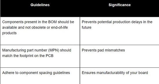
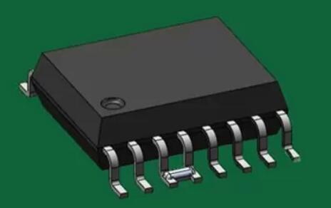
Component Orientation With Polarity Markings
Component orientation is one of the most important factors to be considered during the pre-assembly stage. For a hassle-free assembly, it is essential to follow clear and explicit techniques of orientation. Just as an example, consider diodes, which will have some definite polarity. Make sure the schematic symbol and silkscreen have a proper polarity marking that will be visible after placement. This will make the inspection process easier, and it makes testing or debug easier.
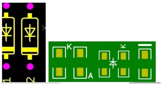
The symbol can be positioned between the two pins for through-hole parts, but it should be placed beside the device for surface-mount parts. Since these symbols can take up a lot of space, a bar above the cathode pad or a simple indication of A (anode) or K (cathode) would suffice for HDI boards.
Always group similar components and try to place them with the same orientation if possible. This facilitates a quick assembly process. For instance, all QFPs can be placed in a row with pin 1 at the same corner for each IC.

Spacing Requirements
Spacing between the components affects the time frame requirements of the PCBA process. In this section, we will have a look at recommended spacing standards to ensure the quality of the assembly process.
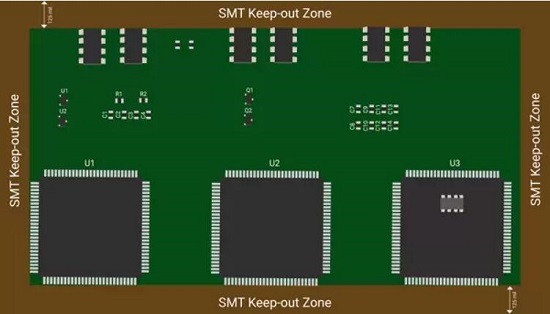
Part-to-Edge Spacing
Part-to-edge spacing is the distance from a given component on the board to its edge. This factor plays an important role during depanelization. During this process, the components near the board edge will be subjected to stress that might affect solder joints. We recommend a 125 mil clearance between the board edge and the SMD placed on the top side of the circuit board, but your fabricator might provide different allowances in their process.
Sometimes, manufacturers further increase the component-to-board edge spacing on the lower side of the board. This reduces the possibility of SMT component damage during the application of solder paste.
Copper traces can also be routed closer to the edge of the board. This allows a solder mask gap and prevents pad encroachment. Traces, copper pour, and manually inserted parts must be spaced at least 10 mils from the board's edge. Castellated holes are a type of design that requires copper plating at the board edge. To achieve the desired copper plating, such designs will require additional expense and lead time.
Part-to-Hole Spacing
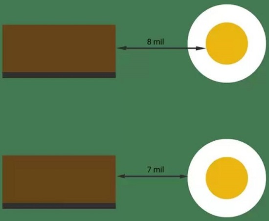
Part-to-hole spacing should be considered for both vias and through-hole components. It determines the minimum spacing between a component pad/body and the holes. Such spacing consists of two specific factors that must be met in order to achieve a high-quality assembly.
1.Part-to-hole wall: This is measured from the actual hole edge to the pad edge. This is also known as drill-to-copper distance. The minimum spacing required is around 8 mils.
2.Part-to-annular ring: This is measured from the edge of the hole’s annular ring to the pad edge. The minimum spacing required is around 7 mils.
Part-to-hole spacing
IPC assembly standards
Here are some of the other IPC assembly standards your CM will stick to while assembling boards.
1.IPC-A-600: IPC-A-600:commonly known as IPC-600, specifies the level of acceptance criteria for each product category. It defines the desirable, permissible, and non-negotiable requirements of the boards.
2.IPC/WHMA-A-620C: It describes the standard for materials, procedures, tests, and acceptability criteria for cable and harness assemblies.
3.IPC-A-630: It defines the standards for electronic enclosures. This standard is employed when your CM assembles and carries out the inspection process.
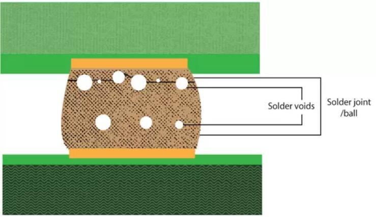
Common Assembly Defects
This section details the defects and issues that occur most frequently during PCBA. Manufacturers employ many quality control methods to avoid these defects, and some of those methods are mentioned in the subsections below.
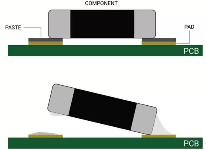
Tombstones
A tombstone, also known as the Manhattan effect, refers to the case where an SMD component is partially or entirely peeled off of its landing pad. This is most common in small SMD passives (0603 or smaller packages) and it occurs due to force imbalances during reflow soldering.
Ways to prevent tombstoning:
1.Ensure high component accuracy and a high preheat temperature.
2.Avoid exposures to high temperatures and humidity.
3.Extend the soak zone to balance the wetting force on both pads before the paste reaches the molten state.
Solder Bridging
Solder bridging occurs when the solder is applied between two conductors that should not be electrically connected. These undesired connections are referred to as shorts.
Ways to prevent solder bridges:
1.Ensure that the metal content in the solder paste is at least 90%.
2.Align the stencil apertures accurately and reduce their size by 10%.
3.Secure an appropriate reflow profile.


0users like this.
