

Categorie

Silkscreen on PCB
Silkscreen on PCB
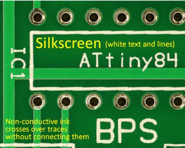
The Silkscreen is the topmost layer of a circuit board which is used as a reference indicator for placing components on a PCB Board. It requires a specifically formulated ink whose standard color is white, but it can also be Red, Black, Yellow, Blue and a number of other colors.
The silkscreen is used to specify useful information on the PCB board that can help/assist users during assembly. It is used to mark component values, part numbers, test points, polarity etc.
What is the purpose of using a silkscreen layer?
The silkscreen is not applied to PCB boards by default. A customer has to ask for this and there is usually an additional charge for applying a silkscreen on the board. Here are some important benefits to opt for the silkscreen layer:
1.It helps the engineers and technicians identify test points on the PCB board. This way they know where to take measurements from and helps when trouble shooting.
2.It can be used to outline where components need to be placed on the board, this way users will not users forget to place components on the board.
3.The silkscreen coating also helps with the warning symbols which are generally used to indicate the higher parameter values such as Voltage, Current and Power.
4.It can be used to specify values of inductors, resistors and other components reducing the probability of placing a component with an incorrect value on the board.
5.Acts as a reference indicator to identify the component type and polarity orientation.
Common Silkscreen Errors and How to Avoid
1.One of the most common errors found on silkscreens is either ignoring to mark polarized parts or not clearly marking them. For electrolytic capacitors, the silkscreen should clearly show which pin is positive. For diodes, it is usually preferred to mark the anode pin with an “A” or “+” and the cathode with a “C” or “-“. Another option for the diode would be to draw the complete diode symbol on the silkscreen so that there is no mistaking which pin is what.
2.Another silkscreen problem can occur when designers use a silkscreen line as a separator between solder pads. This is often seen on two-pin discrete components such as capacitors and resistors, and a silkscreen line is drawn between the two pads. These silkscreen lines may cause the formation of micro solder balls during the solder reflow process. The micro solder balls may then be deposited on the surface of the board and cause inadvertent shorts.
When design the silkscreen layer(s), you can follow the component manufacturer’s recommendations on how to mark their part on a silkscreen. Then submit your Gerber files to your PCB manufacturer who can conduct a free DFM check for your design before an order.
Silkscreen Practices
The first step in creating a good PCB silkscreen is to use the most optimum font sizes and line widths. Font sizes that are too small or are drawn with too wide of a line will end up looking like an ink spot instead of readable text. Line widths that are too narrow may not silkscreen on the board correctly.
Another concern is silkscreen spacing to pads or other PCB objects. Not only will silkscreen be unreadable if it ends up on a pad, but it could also affect the solderability of the board. At MADPCB, we recommend the following values for the best PCB silkscreen results in daily PCB manufacturing and assembly experience:
1.Font size: For best results, use a 1.27mm (50mil) font size and absolutely no smaller than 0.89mm (35mil).
2.Line width: Silkscreen fonts should use no smaller than 0.15mm (6mil) line widths. Keep in mind that although wider lines can be used with larger font sizes for company names, part numbers, and other user information, the line widths must be reduced when using smaller fonts for reference designators, pin numbers, and polarity markings.
3.Clearance: Silkscreen should be kept at a minimum of 0.13mm (5mil) from PCB pads and other objects.
The next important step is arranging the different items on the silkscreen. Reference designators should be close to their part and rotated to be easily readable. Unless it just isn’t possible to fit it in, a good practice is to only use two rotations with designators—0 and 90 degrees.
It can be difficult if someone constantly must rotate the board in their hands to read the next silkscreen element. Also, make sure that important silkscreen information is not covered up by placed components. It is very difficult for technicians and inspectors to find components or pin markings if they are covered by the part.
The data should put into silkscreen layer(s) will usually include the following:
1.Reference Designators: Each component and assembled part on the board should have a unique reference designator.
2.Component Symbols: While most components may have a simple rectangle or line to show how they are aligned on the board, some, such as BGA packages, may require more complex symbols to designate their orientation.
3.Pin Markings: Many components will need their first pins marked, and in the case of large components like connectors with hundreds of pins, there may be additional markings as well.
4.Special Markings: In some cases, a silkscreen may contain specific user instructions, such as switch settings or assembly instructions.
5.Documentations: Silkscreens are also used for marking information, such as company names and contact information, the board name and part number, bar codes, date codes, and other information.
As you can see, the silkscreen is much more important to the assembled circuit board than it is often given credit for. Such as, it is critical that PCB designers spend time to ensure it is created correctly. Here are some of the details to keep in mind as you finalize the silkscreen in your PCB design.
There are three main ways to add silkscreen coating on a PCB:
1.Manual screen-printing: This is a process that can be used when line widths are greater than 7 mm and the registration tolerance is 5 mm.
2.Liquid Photo Imaging (LPI): This process provides more accuracy and legibility over manual screening and is used when line widths are greater than 4 mm
3.Direct Legend Printing (DLP): This is the most accurate way of adding a silkscreen, however, it is very expensive.
0users like this.
