

Categorie

GWT’s PCB assembly board Inspection
GWT’s PCB assembly board Inspection
As an ISO9001 certificated PCB Assembly manufacturer, GWT adheres to a thorough quality and process control. The tests and inspections include physical and visual inspections, open & short tests, AOI inspections, X-ray inspection, ,In-Circuit tests,and functional test ect. These PCBA inspection process ensure customers final product meets their design specifications, and also control the whole production lot to high non-defective ratio which reduce the entire lead time.
GWT’s Inspection & Testing Equipment
1.AOI inspection machine
 Figure 01-AOI Testing machine
Usage:100% inspection for every board; To check if any components missing, damage, deviation or opposite assemble.
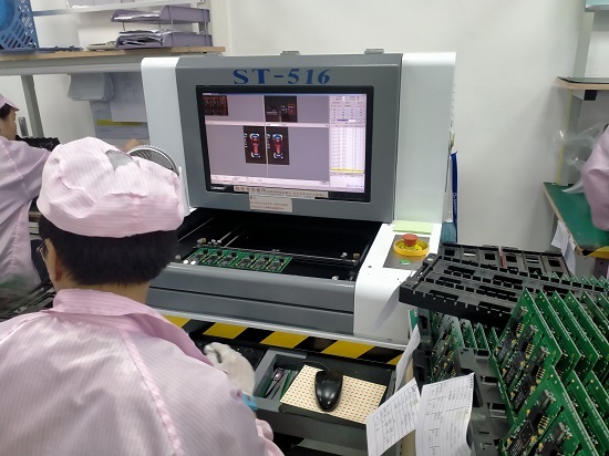
AOI Testing 100% for each board:
--Checks for solder paste conditions
--Checks for components down to 0201 package
--Checks for missing components, offset, incorrect parts, polarity, warp, bent pins…
2.X-Ray Inspection
 Figure 02-X-Ray Inspection
Usage:Inspection BGAs assembling if any fake assemble or shortcuts. Ensure all BAG balls assembled perfectly.
X-Ray Inspection provides high-resolution inspection for your PCB assembly board:
A. Defect inspection in IC encapsulation, e.g.: layer separation, cracking, void, and line integrity.
B.Measuring chip size, measuring line curvature, measuring the proportion of solder area of components.
C.Possible defects in PCB manufacturing processes, e.g.: misalignment, solder bridge and open.
D.SMT solder short, cold solder, component shifted, solder insufficient, solder void inspection and measurement.
E.Defect inspection of open, short or abnormal connections that may occur in automotive wiring harnesses and connectors.
F.Inner rupture or hollow inspection in plastic or metal.
G.Battery stacking uniformity, electrode welding inspection.
H.Seed, biological material inspection etc.
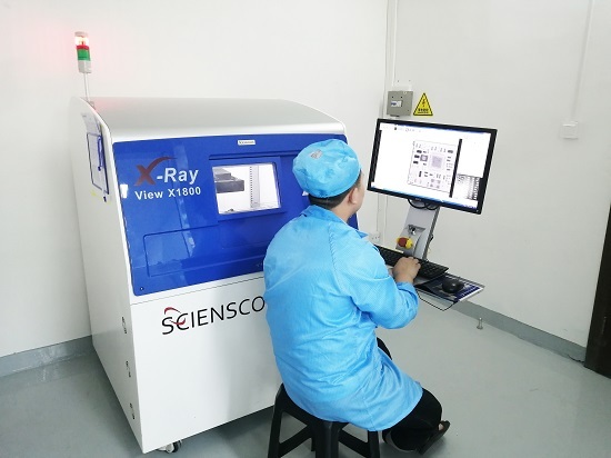
Figure 03-X-Ray Inspection
3.Aging Testing
 Figure 04-Aging testing
--Usage:All PCB aging test methodologies follow a similar procedure: Hold a batch of PCBAs or discrete components at elevated temperature for a certain amount of time (typically multiple hours or days) Test the batch for defects or component failures. Remove the failed parts and test the remaining components/PCBAs.
4.Functional test (FCT)

Functional test (FCT) is used as a final manufacturing step. It provides a pass/fail determination on finished PCBs before they are shipped. An FCT’s purpose in manufacturing is to validate that product hardware is free of defects that could, otherwise, adversely affect the product’s correct functioning in a system application. In short, FCT verifies a PCB’s functionality and its behavior. It is important to emphasize that the requirements of a functional test, its development, and procedures vary widely from PCB to PCB and system to system.
Functional testers typically interface to the PCB under test via its edge connector or a test-probe point. This testing simulates the final electrical environment in which the PCB will be used.
The most common form of functional test simply verifies that the PCB is functioning properly. More sophisticated functional tests involve cycling the PCB through an exhaustive range of operational tests.
0users like this.
