

Categorie
Conventional PCB manufacturing
Conventional PCB manufacturing services
The conventional PCBs have electrical connection on the normal FR-4 material through the vias. After a long-term development, it has evolved from single-layer to double-layer, multi-layer PCBs. Here below we'd like to have a introduction with the regular conventional PCB type:
1.IMPEDANCE CONTROL PCB
Impedance Control PCB refers to the PCB that needs impedance control. Impedance control refers to the “resistance” generated by a certain circuit layer under its high-frequency signal to its reference layer, and its signal must be controlled within the rated range to ensure that the signal is not distorted during transmission. Impedance control is to make each part of the system have the same impedance value, that is, impedance matching.

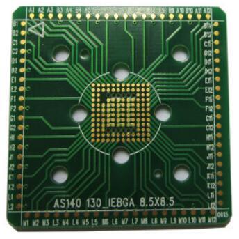
2.Gold Fingers PCB
Among the large-scale use of PCI and optical modules and cable sockets, the gold fingers PCB has been divided into: long and short gold fingers, broken gold fingers, and split gold fingers.
The most common PCB gold fingers design appears on the graphics card and memory stick inside the computer.

Why Choose Gold Fingers PCB?
A. A unique role of PCBA needs to be interconnected with the motherboard but needs to be replaced easily. Design the golden finger and slot connection, similar to the relationship between the power plug and the socket.
B. Because gold has good conductivity and inertness, it ensures the conductive effect without oxidation, and it also ensures sufficient conductivity after frequent insertion and removal of gold.
Gold Finger PCB Design Considerations
A. First ensure that the length, width, position and card slot of the gold finger are fully matched to ensure proper interconnection.
B. The foolproof KEY SLOT designed on the PCB board, the width, height, position and the convexity in the card slot are completely matched.
C. Part of the PCB needs a shorter design of individual fingers, if you can not directly add a wire under the finger, you need to consider how to conduct electricity during pcb gold finger plating.
D. The angle and depth of the beveled edge of the gold finger are the same as the length of the finger. Do not cause the finger to be short or the beveled edge after the beveled edge.
3.Via In Pad PCB
What is Via In Pad?
The holes drilled on the chip pads on the PCB can be referred to as VIA IN PAD. In the manufacturing process, after the via plating, the resin is filled and then the surface is plated and filled, and the via is not visible when the patch is applied.
As we all know, via in pad technology, the PCB plugging process is a process that is produced by the higher requirements of the PCB manufacturing process and the surface mount technology.
The VIA Plugging In PCB Effect has the Following Points
--Prevents short-circuiting of tin from the via through the component surface during PCB over-wave soldering
--Avoid flux remaining in the vias
--Prevent the soldering of the solder balls from over-wave soldering, causing a short circuit
--Prevent surface solder paste from flowing into the hole to cause solder joints, affecting placement
The advantage of the resin plug hole relative to the solder resist plug hole is that the flatness of the pad of the resin plug hole is higher than the flatness of the hole of the solder resist plug, and the disadvantage is high cost and complicated process.
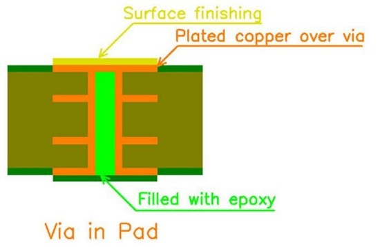
Figure:Via in Pad: Filled with epoxy; Surface Finishing; Plated Copper Over Via.
4.High Tg PCB
When the temperature rises to a certain area, the substrate will change from “glass state” to “rubber state”, and the temperature at this time is called the glass transition temperature (Tg) of the plate. That is, Tg is the highest temperature (°C) at which the substrate remains rigid. That is to say, the ordinary PCB substrate material not only softens, deforms, melts, etc. at high temperatures, but also exhibits a sharp drop in mechanical and electrical properties.
The general Tg of the PCB is 130 degrees or more, the high Tg is generally greater than 170 degrees, and the medium Tg is greater than about 150 degrees.
A PCB board with a typical Tg ≥ 170 °C is called a high Tg board.
The higher the Tg value, the more resistant the sheet is to deformation and the better its dimensional stability. The substrate material of IPC-4101B (2006) standard epoxy/E type fiberglass cloth is divided into three grades according to the height of Tg (commonly known as low, medium and high Tg). It is an important property in the resin of the sheet. It refers to the gradual change of the physical properties of the resin due to the gradual increase of the temperature. It is converted into a viscous state by the amorphous or partially crystalline hard and brittle nature at room temperature, such as glass. The critical temperature is very high and soft in another state like rubber.
5.Edge Plating of Half-hole PCB
The walls of the PTH holes on the PCB are plated with Half-hole formed by smooth and complete metal forming.This type of board has a row of half hole in the PCB, which is characterized by a relatively small aperture, mostly used on the carrier board, as a daughter board of the motherboard, through the half-hole and the motherboard and components The feet are welded together.
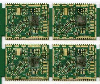
6.Thick / Heavy Copper PCB
There is no exact definition of thick copper in the PCB industry. Generally, the copper thickness ≥ 2oz is defined as Heavy copper PCB. Heavy copper PCB is mainly used in high-current electronic products. High-current electronic products are generally high-power or high-voltage PCBs. They are mostly used in automotive electronics, communication equipment, aerospace, planar transformers, and secondary power modules.
Our thickest copper PCB can make 6 ounces. However, considering the side eclipse factor, copper thickness of more than 3 ounces should pay special attention to the line width of the inner layer.
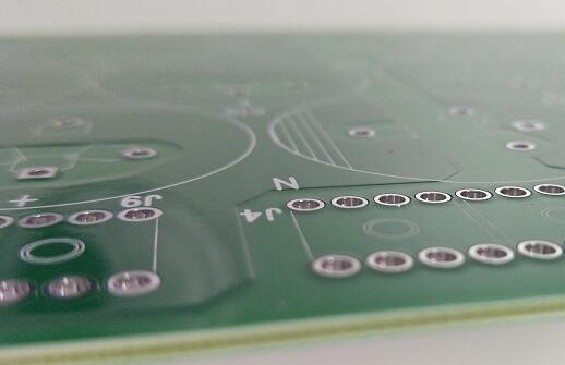
Figure-6OZ copper PCB
The Benefits of Heavy Copper PCBs include: Reduction of Thermal Strain
A. Better current conductivity
B. Can travelers repeated thermal cycling
C. Smaller PCB size due to layering of copper
D. Increased connector site strength
7.Hard Gold PCB
The Application of Hard Gold PCB
Hard Gold PCB is widely used in intelligent AI, entertainment, educational robots or other industrial intelligent equipment to expand and contract, rich in change action, frequent separation and contact of local ports of the device, which requires good wear resistance of the PCB at the contact area of the port. Sexual and not easily oxidized.

0users like this.
